Transistors
Background
What is it?
A transistor is a small semi-conductor that is commonly
found in many electrical devices used today.
Developed as a substitute for vacuum tubes, transistors helped usher in
the miniaturisation of electronics. This
made many conveniences possible like portable computers and mobile phones
(Ross, Shamieh & McComb, 2010).
How can you use it?
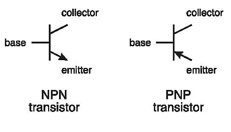 |
| Figure 1.1 |
A typical transistor can have three or more terminals
connected to a head made out of semi-conductor material (Wikipedia, n.d.a). The most common type of transistor is the
Bipolar Junction Transistor (BJT).
This transistor consists of two PN junctions back to back
and has two main arrangements called PNP and NPN as shown in Figure 1.1. The PN junctions mentioned function as two
diodes back to back which denote that the transistor only allows current to
flow in a specific path. As such, this
component is installed in a certain manner.
Why and when would you
use it?
A transistor’s main purpose is to act as a solid state switch
and to amplify electrical signals and power (Brindley, 1999). As a switch, transistors allow one to
control electron flow to suit certain applications and power extra loads if
needed. This would allow complex
circuitries to be made. As an amplifier,
small controlling signals can influence and direct higher electrical output
signals to power motors or loads requiring higher electrical signals (Ross,
Shamieh & McComb, 2010).
Technical Explanation
Transistor Anatomy
| Figure 1.2 |
As mentioned earlier,
the most common form of transistors are the bipolar junction transistors. This type of transistor is commonly made up
of two PN Junctions and will need to be installed in a specific manner in order
for the transistor to work. Figure 1.2
shows the typical legs part of BJT’s termed the Collector (C), Base (B) and
Emitter (E) (Brindley, 1998).
The base is the gate controller device for the larger
electrical supply. This terminal is
therefore responsible for activating the transistor. The collector contains the larger electrical
supply or is the positive lead while the emitter is the outlet of the supply or
the negative terminal (Electronics-Tutorials, n.d.a; Ryan, 2002).
How does this
component work?
| Figure 1.3 |
Next, the two main
types of BJT’s will be explained, the NPN and PNP transistors. As mentioned previously, transistors are
formed and function like two diodes back to back. The direction of flow is dependent on whether
it is NPN or PNP. In Figure 1.3, the NPN
transistor has two N-type substrates and one P-type substrate connected by a
junction. In the same figure, PNP has
the opposite trend with one N-type substrate and two P-type substrates
connected by a junction.
To help with visualising the operation, refer to Figure
1.4. In an NPN transistor, the voltage
of the base must be more positive than the emitter. The collector, in turn, must be more positive
than the base. The emitter will then
supply the electrons (Electronics-Tutorials, n.d.a).
In more detail, with the base being more
positive in a forward bias state in the B-E region, electron holes are pushed
outward to the B-E region as electrons from the emitter meet with the holes and
combine. This allows allow electrons
from the emitter to flow to the base.
The collector will then pull the electrons from the base as it is more
positive (Ross, Shamieh & McComb, 2010).
| Figure 1.4 |
This will activate
the junction and allow large current to flow through the transistor from
collector to emitter (C-E). Therefore
the smaller current running from the base-emitter (B-E) will activate the C-E
junction and allow a bigger current to flow in it (Electronics-Tutorials,
n.d.a).
Next the PNP transistors contain the same terminals but it
is wired slightly differently as current biases are now reversed. This results in the base voltage being more
negative than the emitter as current flows out of the base instead. The emitter, connected to the supply voltage,
is therefore more positive than the collector and the base
(Electronics-Tutorials, n.d.b).
In more detail, the emitter region is heavily doped with
holes while the base is lightly doped.
Once forward biased at the E-B junction, positive supply will push the
holes in the emitter to the E-B junction while the negative base will also push
its electrons to meet the holes at the E-B junction which allows the electrons
and holes to combine (Bhatia, n.d.). The
base region will have an influx of holes and most of these holes will then flow
to the collector region as they will be attracted to the larger negatively
charged collector (Bhatia, n.d.). A
small number of holes also flow out of the base terminal. This would then allow a larger current to
flow from emitter to collector (Electronics-Tutorials, n.d.b).
In summation, NPN transistors sources its current through
its base terminal while PNP transistors sink or grounds current through its
base. NPN transistors also rely on
electrons as the carriers while PNP transistors employ the holes as its
carriers (Electronics-Tutorials, n.d.b).
Now that the basic operation has been explained, a look into
how NPN transistors main functions as a switch and as an amplifier will be done
to further understand its workings.
 |
| Figure 1.5 |
As a switch, the NPN transistor
can operate in two states, saturation and cut-off, which are illustrated in
Figure 1.5. The ability to act as a
switch can allow the transistor to control motors and other loads
(Electronics-Tutorials, n.d.c).
When the transistor is operating in a saturated state, the
switch would be fully on. The
emitter-base and collector-base a forward biased. When the transistor is fully saturated, the
VCE is near zero and the base to emitter (Ib) has sufficient current flow which
subsequently allows large current flow from the collector to occur. The transistor would then function as a
“closed switch” (Electronics-Tutorials, n.d.c).
In cut-off mode, the emitter-base and the collector base
regions are reverse biased. The VCE will
become very high, nearing supply voltage. The current flowing in Ib is zero and
as a result of this, no current will pass from the collector and the transistor
would operate as a “open switch” (Electronics-Tutorials, n.d.c).
In addition, both of these states have low power dissipation
(Electronics-Tutorials, n.d.c).
 |
| Figure 1.6 |
The other main
function of a transistor is to amplify electrical signals, which is shown on
Figure 1.6. To amplify small signals,
the transistor must enter a state called the active region. In this region, emitter-base is forward
biased while collector-base is reverse biased.
High power dissipation and high VCE is observed in this region. What results is the transistor being able to
amplify smaller signals to large currents.
How much the current is amplified is is explained through the beta β =
Ic/Ib equation which states that the current multiple gained is the ratio
between the collector current and base current.
Therefore how much larger the collector current becomes is affected by a
change in the base current (Oregon State, n.d.).
Test Procedure
Identifying terminals
and the kind of bipolar junction transistor
Testing for the type of BJT a digital multi-meter is needed
to help identify the terminals. Because
transistors normally function as two diodes back to back, diode test mode is
used. Place the red lead as the common and
work the black probe at each of the other two terminals to see if you get a
reading (All About Circuits, n.d.).
Terminal Test Results
|
|
Terminal and (Probe)
|
Reading
|
1 (+) to 2 (-)
|
OL
|
1 (+) to 3 (-)
|
OL
|
2 (+) to 1 (-)
|
0.713V
|
2 (+) to 3 (-)
|
0.711V
|
3 (+) to 1 (-)
|
OL
|
3 (+) to 2 (-)
|
OL
|
In the first test, with the red probe connected randomly to
the leg 1, an open loop reading was attained from legs 2 and 3. This denotes that there is no flow from legs
1 to 2 and legs 1 to 3.
Next is to test from leg 2.
Legs 2-1 and 2-3 yielded a 0.713V and 0.7.11V readings respectively. This helps indicate that there is a forward
flow between the aforementioned combinations.
The higher reading shows the emitter and the lower one the collector.
Lastly, checking legs
3-1 and 3-2 showed both open loop readings.
The initial results point it to be an NPN transistor but to be sure,
switching the negative probe to leg 2 and making sure an open loop reading is
seen to decisively conclude whether the diode is in fact an NPN transistor.
 |
| Figure 1.7 |
In conclusion, we found that B-E voltage was
0.713V while E-B voltage had an open loop reading. B-C voltage was 0.711V and C-B had an open
loop reading. C-E and E-C had also had
open loop readings which confirmed the transistor as an NPN type. Table 1.1 shows the results.
Looking up the Figure 1.7 shows the back to back diode forms
of NPN and PNP transistors. Therefore
readings will have biases in the respective directions of the illustrations to
identify the type of transistor.
Testing for proper
function
Utilising the same test procedure to check for the kind of
transistor above is also useful to check for transistor function as well. If all terminals had readings of 0.713V then
the transistor is not functioning properly as forward and reverse flow is
present (All About Circuits, n.d.).
Readings if connected
to a circuit
If the NPN transistor was to be put into a basic circuit,
the legs must be connected properly with the base and collector after certain resistors
and the emitter to ground. Figure 1.8
shows a sample schematic of a transistor wired up.
 |
| Figure 1.8 |
In this circuit,
there is a 15V power supply with a 1K (R2) resistor connected to the collector
and a 10K (R1) resistor connected to the base.
The emitter then connects to ground.
Available voltage readings before R1 and R2 would be close to 15V. After R1, the available voltage was 0.6V
while after R2 was 0.2V. After the
emitter the voltage measured was close to 0V.
These are typical readings that you would find in this circuit.
Problems
 |
| Figure 1.9 |
Utilising Figure 1.9
as reference of a sample faulty circuit, if there was a breakage in the wiring
before the base terminal’s resistor, this would result in a 0V reading after
that resistor and its subsequent base. If this was to happen, then there would be no smaller
current to activate the larger collector current and no current flow would
result from the collector-emitter region.
The voltage drop from the collector-emitter region would see a voltage
drop of the whole supply voltage.
In another example, if the transistor itself was faulty with base-emitter region short circuited, voltage drop readings in the base-emitter region would be 0V. Because the base-emitter region was at 0V, the insufficient voltage and current would not be enough to activate the junction and thus, no current would flow from the collector to the emitter and that region would see a supply voltage drop and results in a cut-off like state where the transistor is off.
For a different example, if this time the collector-emitter
was to have an open circuit, the collector-emitter would see a drop of the
entire voltage supply while the base-emitter region will see a normal 0.7V
drop. The result is though current is
able run through the base-emitter region, but because there is an open circuit
in the collector-emitter region, no current is able to pass through.
Reflection
Learning about transistors further deepened my understanding
of how electrical components work theoretically. In addition to strengthening my theoretical
and logical framework, I also learnt how it can be applied to different
situations to help amplify or act as a switch to activate motors and other such
loads.
With these important main functions, all able to be
performed in a very compact but well thought out and constructed component, its
contributions to modern electronics should not be overlooked. It helped make computers smaller than ever
and phones portable. Electronic machines
became smaller as a result and this is a big contribution of transistors.
Partaking in the experiments, measuring voltage drops and
available voltages also helped me in understanding the trends that occur in a
working circuit. This also helped me in
understanding how potential problems can result and what readings they may
give. It was a worthwhile and important
component to learn and no doubt, I will come to use this component a lot more
in the future and in more varied and complex ways.
Reference List
All About
Circuits. (n.d.). Meter check of a
transistor. Retrieved March 17, 2013 from http://www.allaboutcircuits.com/vol_3/chpt_4/3.html
Bhatia, A.
(n.d.). Introduction to transistors. Retrieved
March 17, 2013 from http://www.cedengineering.com/upload/Transistors.pdf
Brindley, K. (1999). Starting
electronics (2nd ed.).
Oxford: Newnes.
Electronics-Tutorials.
(n.d.a). The NPN transistor. Retrieved
March 15, 2013 from http://www.electronics-tutorials.ws/transistor/tran_2.html
Electronics-Tutorials.
(n.d.b). The PNP transistor. Retrieved
March 15, 2013 from http://www.electronics-tutorials.ws/transistor/tran_3.html
Electronics-Tutorials.
(n.d.c). Transistor as a switch. Retrieved
March 16, 2013 from http://www.electronics-tutorials.ws/transistor/tran_4.html
Oregon State.
(n.d.). BJT regions of operation. Retrieved
March 17, 2013 from http://web.engr.oregonstate.edu/~traylor/ece112/lectures/bjt_reg_of_op.pdf
Ross, D., Shamieh, C., & McComb, G. (2010). Electronics for dummies. Cornwall:
Wiley.
Ryan, V. (2002). Transistors. Retrieved March 15, 2013
from http://www.technologystudent.com/elec1/transis1.htm
Wikipedia.
(n.d.). Transistors. Retrieved March
15, 2013 from http://en.wikipedia.org/wiki/Transistor